Lou D's Voltage Regulator
for Excited-Field Alternators
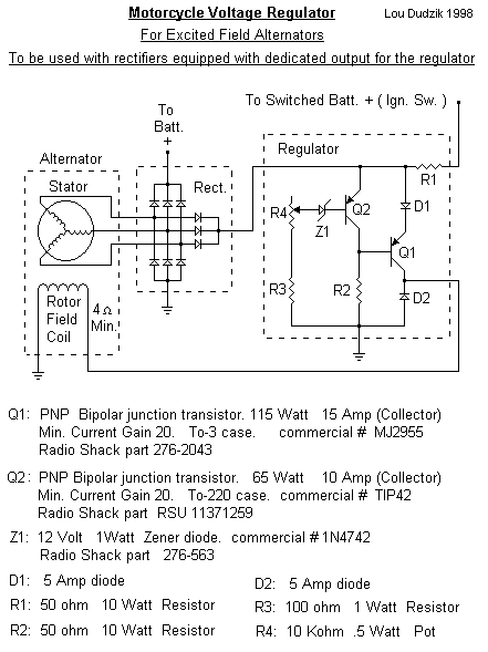
For Yamaha RD350 and YR5
(Adaptable to other bikes using excited-field alternators)
Intro:
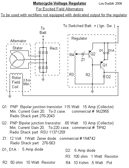
This project is a voltage regulator for motorcycles. It was originally designed for a Yamaha YR5 motorcycle. It is also compatible with some Yamaha RD 350 motorcycles. It is generally compatible with any motorcycle equipped with an excited-field alternator with a minimum field coil resistance of 4 Ohms.It should be used with a rectifier designed with a dedicated, positive-voltage tap to power the field coil. This prevents the battery from draining quickly at low RPMs. (I also have a similar design for rectifiers which do not have the dedicated tap for powering the field coil. It is at the bottom of this page. Most of this discussion is relevant for both designs.)
The main goal of the design was to be simple and easy to build with parts available at Radio Shack.
There is an accompanying drawing which should be referred to during the analysis of the circuit.
Circuit Analysis:
This is the analysis of the regulator portion of the circuit drawing.
Overview:
When the voltage at the rectifier output is below 14.5 Volts, the regulator applies current to the field coil of the alternator. When it is above 14.5 Volts, the regulator "turns off" the field coil current. Because the field coil is an inductor, it does not turn off and on instantly, it takes time. This is advantageous because it allows time for the regulator's transistors to go into saturation or cutoff, completely. This reduces the heat in the transistors and reduces power waste. It does, however, allow the output to briefly surge above 14.5 V, up to approximately 15 V.When the rectifier's output is below 14.5 Volts, Q2 is in cutoff. This means the base voltage of Q1 is allowed to drop below the emitter voltage of Q1. Q1 is "on" and current flows through D1 and Q1 to the field coil.
As the current increases, so does the output of the alternator and rectifier (provided that the engine is turning with adequate RPM). When the rectifier's output exceeds 14.5 Volts, Q2 turns "on". This causes the base voltage of Q1 to increase thus turning Q1 "off". D1 is needed to make sure that the emitter-base junction of Q1 will be fully reverse-biased when Q2 is "on". It does this by dropping the emitter voltage of Q1 by about 1 Volt.
When Q2 turns "off", the inductance of the field coil causes its current to drop slowly as opposed to stopping instantly. D2 is used to provide a path to drain the current. Without it, a large induced voltage would occur at Q1, possibly causing damage to Q1.
Q2 is controlled by R3, R4, and Z1. When the recifier output is above 14.5 Volts, Z1 begins to conduct in Zener mode. This turns on Q2. R4 is adjustable to fine tune the voltage at which the regulator will operate.
It will be assumed that the maximum steady output voltage from the rectifier (referred to as Vr from now on) will be about 15 Volts with allowable spikes of 20 Volts.
It will be assumed that the minimum resistance of the field coil will be no less than 4 Ohms.
This means the maximum field coil current can be found :Max. Field Coil Current = (Vr - V of D1 - V Q1 saturated) / R of field coil
= (15 - 1 - .3) / 4
= 3.425
Max. Field Coil Current = 3.425 Amp
Selecting D1:
D1 must handle the full current of the field coil as found above.Current in field coil = 3.425 A
For safety and availability, D1 will be a 5 Amp diode.
D1: 5 Amp diode
Selecting D2:
Because D2 will also handle the full current of the field coil (but only briefly), it will be the same as D1.D2: 5 Amp diode
Selecting R1:
Under certain conditions, such as low RPM or when the engine is stopped, the battery will supply the current to the field coil. R1 limits this current from the battery. Without it, the battery would drain quickly. R1 allows enough current to begin exciting the alternator. When the RPMs increase, the alternator produces the current to fully excite itself. This is done through the secondary, positive output from the rectifier. R1 is selected to limit the current to about .25 A. In this situation, the battery voltage will usually be around 12 Volts. (These are rough estimates, but are adequate for the purpose.)Voltage on R1 = ~ 12 V
Current in R1 = ~ .25 A
R1 = 12V / .25 A = ~ 50 Ohm
R1 = 50 Ohm
Power in R1 = 12 V x .25 A = 3 W
For safety and availability, use 10 WR1: 50 Ohm, 10 W
Selecting Q1:
The maximum field current is also the maximum collector-current for Q1 (about 3.5 Amps).The maximum steady power dissipation in Q1 will occur when the transistor is in the active region. Through the use of calculus, which will be skipped here, the maximum power dissipation occurs when the voltage drop in the transistor is equal to the voltage drop in the load (field coil). That value will be approximately 7 volts.
The current in this case is found by:
current = 7 V / 4 Ohm = 1.75 AmpThe power is then 7 V x 1.75 Amp = 12.25 Watts.
The most the transistor should need to dissipate, then, is 12.25 Watts. However, due to operating in a hot environment, a large safety margin will be allowed for. 50 Watts should be adequate, but more would be nice.
For availability and safety reasons, the transistor chosen for Q1 will be an MJ2955. It has an advertised minimum gain of 20, maximum collector-current of 15 Amp, and can dissipate 115 Watts.
Q1: MJ2955
A small heat sink should be used for Q1. This can just be a simple plate of aluminum with about four square inches of surface area.
Selecting R2:
The purpose of R2 is to limit the base-current of Q1.
Using the maximum collector-current of Q1 ( 3.5 Amp), and the minimum gain, the required base-current can be found :Saturation base-current = 3.5 Amp / 20 (current gain) = .175 Amp
This is the absolute minimum base-current to achieve saturation. Saturation is desired in order to reduce heat and power waste in the collector-emitter circuit. In case the actual gain is less than the advertised value, and to come up with a readily available resistor value for R2, the minimum base-current requirement will be increased to .266 Amp. This is called overdriving the transistor and will ensure saturation is achieved. Veb is the emitter-base voltage of Q1 and is about 0.7 V. V of D1 is the voltage on D1 and is about 1 V.
The base current for Q1 in saturation is .266 Amp. R2 can be found as follows:
The voltage on R2 = 15V - V of D1 - Veb of Q1 = 15 - 1 - 0.7 = 13.3 VR2 = voltage on R2 / base current of Q1 = 13.3 V / .266 A = 50 Ohms
The power of R2 is found as follows:
There are actually two cases that need to be taken into account.When Q2 is "off", the only current is that through Q1.
Power = Voltage on R2 x Current = 13.3 V x .266 A = 3.5 WattWhen Q2 is "on", the voltage on R2 (and the current) is slightly higher.
The emitter/collector voltage of Q2 in saturation is about .3 Volts.
Thus, the voltage on R2 = 15 - .3 = 14.7 V
The current is 14.7 V / 50 Ohm = .294 Amp
(This is also the collector-current of Q2)
Power = 14.7 V x .294 Amp = 4.3 WattFor safety, a 10 Watt resistor will be used.
R2: 50 Ohm, 10 Watt
Selecting Q2:
To turn off Q1, Q2 must raise the base voltage of Q1 to within 1.7 Volts of Vr. Q2 can easily do this by going into saturation. In saturation, the collector-emitter junction will be around 0.3V. This means the base of Q1 will be at .3V below Vr, therefore Q1 is off.In finding R2, the maximum collector-current of Q2 was also found. It is .294 Amp.
The maximum steady power dissipation in Q2 will occur when the transistor is in the active region. Through the use of calculus, which will be skipped here, the maximum power dissipation occurs when the voltage drop in the transistor is equal to the voltage drop in the load. That value will be approximately 7 volts. (Here, the load is R2).
The current in this case is found by:
current = 7 V / 50 Ohm = 0.14 AmpThe power is then 7 V x 0.14 Amp = 0.98 Watt.
The most the transistor should need to dissipate, then, is about 1 Watt. However, due to operating in a hot environment, a large safety margin will be allowed for. 20 Watts should be adequate, but more would be nice.
For availability and safety reasons, the transistor chosen for Q2 will be a TIP42. It has an advertised minimum gain of 20, maximum collector-current of 10 Amp, and can dissipate 65 Watts.
Q2: TIP42
Sense Circuit:
Z1, R3, and R4 make up the voltage-sense circuit.Z1 is a Zener diode. It's purpose is to start conducting when Vr exceeds 14 V. Generally speaking, Zener diodes are designed to start conducting when their threshold voltage has been exceeded. In practice, they start conducting a small leakage current well below their threshold voltage. Also, the threshold voltage varies slightly from diode to diode. Because of this, an adjustment is incorporated. The adjustment also compensates for gain variances in the transistors.
R4 is used to fine tune the circuit to the desired voltage.
R3 is a current limiter to protect the Zener diode and R4.
In order to decide on values for R4 and R3, three limits must be found. The first limit occurs when both transistors have minimum gain. The second limit occurs when both transistors have high gain. The third limit is that of power dissipation in the Zener diode.
The first step is to determine the base-current of Q2 in order to turn Q1 off when both transistors have low gain. (Assume both transistors have a gain of 13.5.) (13.5 is chosen for convenience)
Field coil is 4 Ohm. Voltage applied to field coil is approximately 12 V.
Q1 collector-current = 12V / 4 Ohm = 3 Amp
3 Amp / 13.5 / 13.5 = .019 Amp
Q2 base-current upper limit is .019 AmpThe next step is to determine the base-current of Q2 in order to turn Q1 off when both transistors have high gain. (Assume both transistors have a gain of 100.)
Field coil is 4 Ohm. Voltage applied to field coil is approximately 12 V.
Q1 collector-current = 12V / 4 Ohm = 3 Amp
3 Amp / 100 / 100 = .0003 Amp
Q2 base-current lower limit is .0003 AmpThe next step is to select Z1.
Selecting Z1:
Z1 is selected as a 1N4742. It is readily available and can handle 1 Watt. It's advertised threshold is 12V.In order to find R3 and R4, some more information is needed about the 1N4742 Zener diode. When Z1 is conducting the current limits as calculated above, the value for the voltage applied to Z1 is needed.
Through experimentation, the following characteristics were measured on a typical 1N4742 Zener diode:
It conducts .019 Amp at 11.9 Volts.
It conducts .0003 Amp at 11.54 Volts.Z1: 1N4742
Selecting R3:
In order to find the value for R3, R4 will be set to zero Ohms. This is the condition when both transistors have minimum gain. Therefore, the Q2 base-current is .019 Amp, and Vz is 11.9 V. Vz is the voltage across Z1. Veb Q2 is the base-emitter voltage of Q2. The voltage on R3, when Vr is 14.5 V, is found as follows:voltage on R3 = Vr - Vz - Veb
= 14.5 - 11.9 - 0.7
= 1.9 Vcurrent = .019 A
R3 = voltage / current
= 1.9 / .019
= 100 OhmsFinding the power in R3 requires another experimental value for current and voltage in Z1. This value was measured specifically for this calculation.
Vz is 12.0 V at .023 A.
The maximum power in R3 is when R4 = 0, and Vr = 15 V.voltage on R3 = Vr - Vz - Veb
= 15 - 12.0 - 0.7
= 2.3 VThe current is .023 A.
Power in R3 = voltage x current
= 2.3 V x .023 A
= .05 Watt0.05 Watt seems low enough to manage at first glance, but because Z1 is not linear, the power in R3 can vary greatly with Vr. Therefore, R3 is recommended at 1 Watt. It should be at least .5 Watt.
R3: 100 Ohm, 1 Watt
Selecting R4:
R4 is variable, but the maximum value is determined by assuming the gain in each transistor is high (100). The base-current in Q2 is .0003 Amp and Vz is 11.54 Volts. The voltage on R3 is negligible.The voltage on R4, when Vr is 14.5 V, is found as follows:
voltage on R4 = Vr - Vz - Veb
= 14.5 - 11.54 - 0.7
= 2.3 Vcurrent = .0003 A
R4 = voltage / current
= 2.3 / .0003
= 7667 OhmsR4 will be selected as 10 K Ohms.
Since R3 and R4 are the only resistances in the Q2 base circuit, the maximum power dissipation in R4 occurs when R4 = R3 (100 Ohms). When R4 is 100 Ohms, the total power will be half that of R3 alone. Half of that will be dissipated in R4. Therefore, if R3 is rated at 1 Watt, R4 can be rated at .25 Watt. For safety and availability, .5 Watt will be selected.
R4: 10 K Ohm, .5 Watt potentiometer
Power in Z1:
The last step is to verify that 1 Watt is sufficient for Z1. R4 will be set to zero Ohms. (R3 is 100 Ohms).The voltage on R3 = Vr - Vz - Veb
= 15 - 12 - .7
= 2.3 VThe current in R3 = 2.3 V / 100 Ohm
= .023 AThe current in Z1 = current in R3
The power in Z1 = Vz x current in Z1
= 12 x .023 A
= 0.276 Watt1 Watt is sufficient for Z1.
Conclusion:
This circuit was built and used on a Yamaha YR5 and an RD350. After installing the regulator, the only adjustment required is to turn the voltage adjustment pot to get about 14.5 volts with adequate RPM. After the adjustment is made, the circuit can be sealed into a container of some sort. The transistors should be mounted securely and isolated electrically. Q1 should be mounted on a small heatsink. This can just be a simple plate of aluminum with about four square inches of surface area.
It has been in use for over 5 years with no problems.