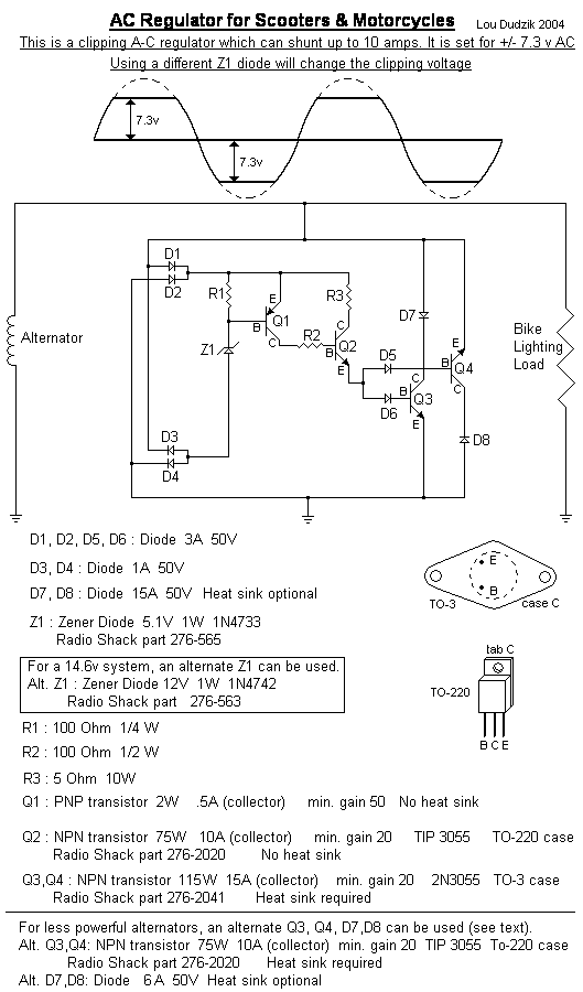
AC Regulator
For 6 volt scooters with AC powered lights
(Adaptable to other bikes)
AC regulator for 6v scooters with AC powered lights
Overview:
The purpose of this project is to design a voltage regulator for the lighting system of any motorcycle or scooter using an AC system with no battery or other regulator where one leg of the alternator is grounded to the engine. When one leg is grounded, a full-wave rectifier cannot be used, thus a conventional regulator cannot be used. In order to get full power from the alternator, the system must remain in AC operation. Therefore, an AC regulator is needed to prevent excessive voltage from burning out light bulbs. Since 6-volt (7.3v) systems are more common on older scooters, this design will be done for a 6-volt system. However, simply changing one part, as described below, should allow the regulator to work on a 12-volt (14.6v) system.The type of regulator being used is called a clipper. This is because it clips the top and bottom of the voltage waveform. It is similar to a shunting regulator, but instead of shorting the current completely, so the waveform has 0 volts, the clipper shunts the current until the waveform is limited to 7 volts. This is necessary since there is no battery (or capacitor) to maintain voltage to the load (in this case, lights). With a complete short, the waveform would only consist of small-duration spikes of voltage. A clipper provides long-duration, clipped waveforms which contain much more energy without excessive voltage.
Circuit Description:
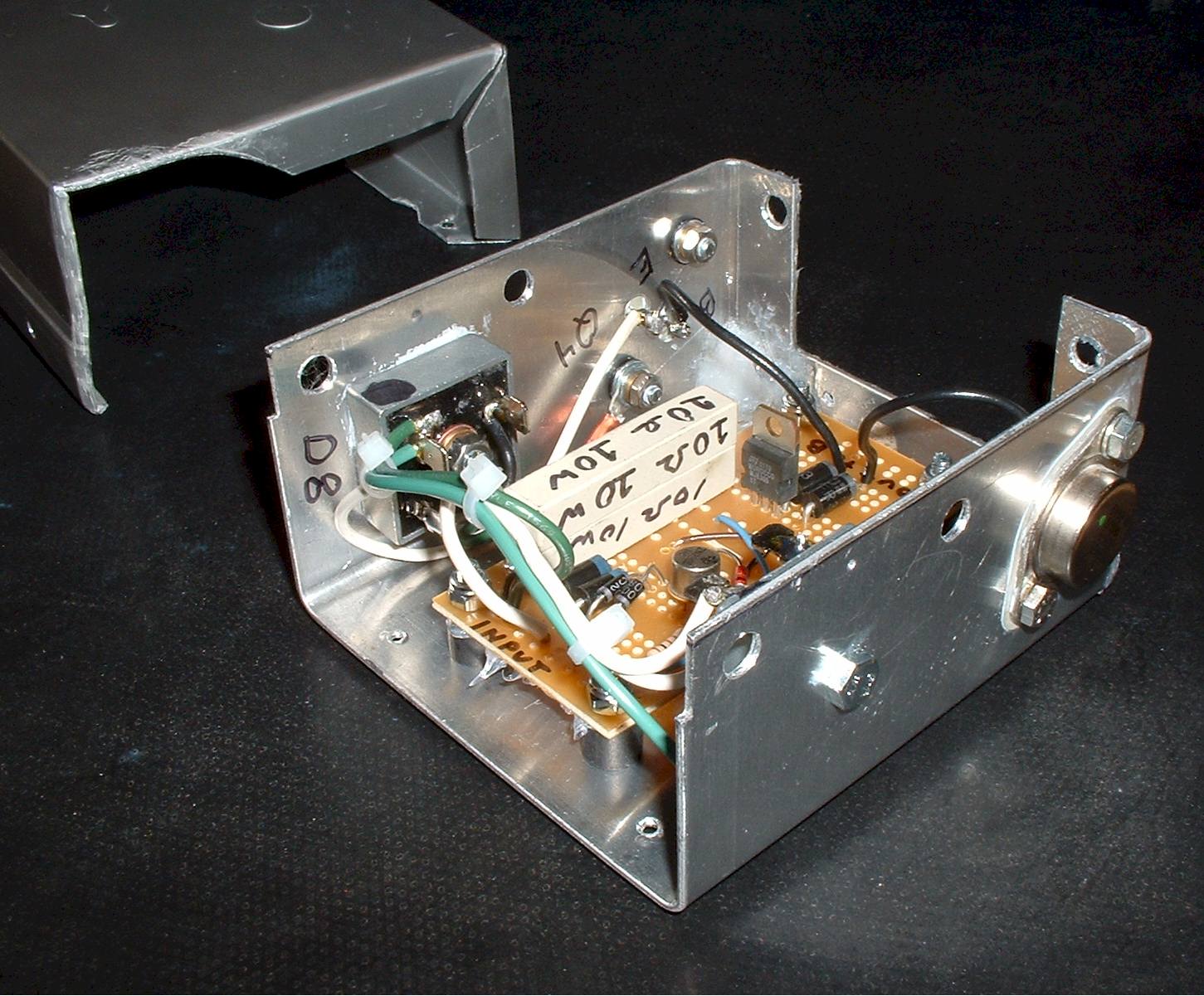
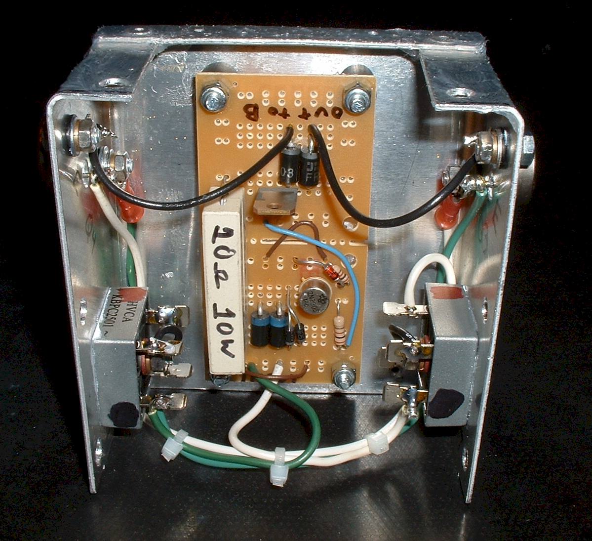
(Please refer to the schematic drawing for the description.)
The alternator’s output fluctuates with engine RPM. Excessive voltage could cause the bulbs to burn out. The purpose of the clipper is to limit the maximum allowable voltage. It does this by detecting the system voltage and shunting current away from the load (in this case lights) to stop the voltage from increasing past a set voltage (in this case, about 7v). A voltage detection circuit is used such that when the system voltage is less than 7v, the power transistors are off. When the voltage starts to rise above 7 volts, the detection circuit turns on Q1, which turns on Q2, which turns on either Q3 or Q4 depending on the polarity of the AC voltage at the time. Q3 or Q4 shunts current to stop the voltage from increasing. If alternator output increases, the shunt-current increases, but the system voltage does not. It is estimated that the maximum shunt-current required to maintain 7 volts should be no more than 10 amps and usually a lot less. This means the circuit will be designed to reliably shunt a maximum of 10 amps. However, an alternate design may be used if it is known that the shunt-current will be less than 5 amps max. This is usually the case. The alternate design simply uses smaller transistors for Q3 and Q4 and smaller diodes for D7 and D8.In order to function for AC operation, one shunt circuit is used for each polarity of the AC voltage. However, to avoid unnecessary redundancy, only one detection circuit is used. D1, D2, D3, and D4 allow for the usage of a single detection circuit. As can be seen, those four diodes actually form a bridge rectifier. However, it is unbalanced since D3 and D4 use less current than D1 and D2. Essentially, the detection (and amplification) circuit receives power delivered by the “bridge rectifier”.
Z1, R1, and Q1 form the detection circuit. R1 is used to bias the zener diode Z1 into its linear range. R1 ensures there is an idle-current of about 7ma through Z1 before the base of Q1 conducts any current. Since R1 is parallel to the e-b junction of Q1, it will only have a maximum of .7 volts on it. Therefore, the maximum current through R1 will be the idle current. Any other current through Z1 will have to go through the e-b junction of Q1. Any current increase through Q1 will have minimal affect on the voltage on Z1 since Z1 is a zener diode. However, the increase of current through Q1 will cause a large increase in the shunt-current through Q3 or Q4. The increase in shunt current will prevent the system voltage from going any higher. This means the zener voltage of Z1 will determine the final system voltage. To provide for a 14v system, only Z1 needs to be changed.
Q2, R2 and R3 are an intermediate stage used to drive Q3 and Q4. This stage is required since Q1 would not have the power to drive Q3 and Q4 directly.
D5 and D6 are used to isolate Q3 and Q4 from each other.
D7 and D8 are used to protect Q3 and Q4 respectively against collector-emitter reverse voltage conditions when the polarity is reversed. D7 and D8 must handle full shunt-current, so they must be able to handle at least 10 amps reliably.
To select the components for this project, it is perhaps best to analyze the circuit in reverse; starting with D7 and D8 and working towards D1 and D2.
Selecting D7 and D8:
D7 and D8 must each handle the full shunt-current so they must be able to handle 10 amps (with a 50% duty cycle). For safety, they will be selected as 15a, 50v diodes. The 50v PIV (peak inverse voltage) should be more than sufficient to protect the output transistors (Q3 or Q4). Only 7v (or 14v) is expected.For the optional circuit, which would only handle 5 amps, D7 and D8 could be downgraded to 6a, 50v diodes.
Selecting Q3 and Q4:
Q3 and Q4 must handle 10 amps through the collector-emitter junction. For safety, they will be selected as 15-amp transistors. The power is significant in this design since the transistors will usually be in their active range. The maximum power is as follows:The c-e voltage will be found as:
c-e voltage = system voltage - D7 (or D8) voltage
c-e voltage = 7v - .7v = 6.3vmax power = c-e voltage x max current
max power = 6.3v x 10a = 63wFor safety, 115-watt transistors will be used.
Q3 and Q4 are 15a, 115w transistors. The commercial part number is 2N3055 which comes in a large TO-3 type case. The minimum gain is usually rated at 20 for this transistor.
For the optional circuit, which would only handle 5 amps, Q3 and Q4 could be downgraded to 10a, 75w transistors. The commercial part number is TIP 3055 which comes in a more convenient TO-220 case. The minimum gain is usually rated at 20 for this transistor.
Selecting D5 and D6:
D5 and D6 are to isolate Q3 and Q4 from each other. Therefore, they need to block the reverse voltage through the e-b junction. 50 volt PIV should be more than adequate.To determine the current requirements for D5 and D6, the base currents for Q3 and Q4 need to be determined. Since the maximum current through Q4 or Q3 is specified as 10 amps, and the minimum gain is 20 for Q3 and Q4, we can find the base current as follows:
First, it will be assumed the minimum gain is actually as low as 10.
Base current = collector current / gain
Base current = 10a / 10 = 1aD5 and D6 need to handle 1 amp reliably. For safety, 3-amp diodes will be used.
D5 and D6 are 3a, 50v diodes.
Selecting R3:
R3 acts as a current limit for the Q3, Q4 base-circuit. R3, arguably, may not necessarily be needed. If nothing else, it may at least ensure that Q2 doesn’t need a heat sink since, in a worst-case scenario, most of the voltage drop in the base-circuit will be on R3 instead of on Q2. (This is not necessarily true for a 14.6v system.)The most base-current is delivered when Q2 is in saturation. For the sake of determining R3, it will be assumed that Q2 is in saturation when delivering 1 amp (the maximum expected base-current for Q3 or Q4). Using this, a minimum value for R3 can be determined.
If Q2 is saturated, the voltage on R3 is determined as follows:
V on R3 = system volts - D1 volts - Q2 (c-e) volts - D6 volts - Q3 (b-e) volts
V on R3 = 7.3v - .7v - .3v - .7v - .7v
Voltage on R3 = 4.9vThe value of R3 is determined as follows:
R3 = voltage on R3 / current in R3
R3 = 4.9v / 1 amp
R3 = 4.9 ohmsR3 will be selected as 5 ohms.
The power in R3 can be determined as follows:
Power in R3 = voltage on R3 x current through R3
Power in R3 = 4.9v x 1 amp
Power in R3 = 5wFor safety, R3 will be selected as 10w.
R3 is 5 ohm, 10w.
Selecting Q2:
Q2 drives the base of Q3 or Q4 depending on the polarity of the system voltage. It was determined earlier that the base-current of Q3 or Q4 is at most 1 amp. (Since Q3 and Q4 are never simultaneously “on”, 1 amp is the most Q2 needs to flow.In order to determine the power dissipation in Q2, some calculus is required. However, an overly cautious, worst-case scenario can be used to avoid the calculus. The most current Q2 will deliver is 1 amp.
The most voltage Q2 will ever have on it (collector to emitter) can be determined as follows:
(For this, the 14.6v system will be used)
Q2 (c-e) volts = system volts - D1 volts - D6 volts - Q3 (b-e) volts
Q2 (c-e) volts = 14.6v - .7v - .7v - .7v
Q2 (c-e) volts = 12.5vEven though the peak current wouldn’t normally occur with the peak voltage on Q2, these conditions will be used to determine the worst-case scenario power dissipation in Q2.
Power in Q2 = voltage on Q2 x current in Q2
Power in Q2 = 12.5v x 1a
Power in Q2 = 12.5wQ2 should never expect to dissipate more than 12.5w.
Q2 will be selected as a TIP3055 transistor. This is rated as 10a, 75w, with a gain of 20. 75w seems excessively over built, but the transistor will be used without a heat sink, so the rating is in line with what is needed.
Selecting R2:
R2 is a current limit resistor for Q1 and Q2. It will be assumed Q2 has a minimum gain of 20 for the sake of determining R2. Since Q2 is required to deliver at most1 amp (collector-current), the maximum base-current of Q2 is as follows:Base-current = collector-current / gain
Base-current = 1a / 20
Base-current = .05aThe most base-current is delivered when Q1 is in saturation. For the sake of determining R1, it will be assumed that Q1 is in saturation when delivering .05 amp (the maximum expected base-current for Q2). Using this, a minimum value for R2 can be determined.
If Q1 is saturated, the voltage on R2 is determined as follows:
V on R2 =system volts - D1volts - Q1(e-c)volts - Q2(b-e)volts - D6volts - Q3(b-e)volts
V on R2 = 7.3v - .7v - .3v - .7v - .7v - .7v
Voltage on R2 = 4.2vThe value of R2 is determined as follows:
R2 = voltage on R2 / current in R2
R2 = 4.2v / .05 amp
R2 = 84 ohmsFor convenience R2 will be selected as 100 ohms.
The power in R2 can be approximated as follows:
Power in R2 = voltage on R2 x current through R2
Power in R2 = 4.2v x .05 amp
Power in R2 = .21wFor safety, R2 will be selected as .5w.
R3 is 100 ohm, .5w.
Selecting Q1:
Q1 is selected as a PNP transistor. This is opposed to an NPN transistor. Using a PNP transistor here has the advantage of having fewer components in the voltage detection circuit. If an NPN had been used, the current through Z1 would have had to go through the other transistors and diodes. By minimizing the number of components in the path, voltage detection can be more precise.Q1 amplifies the voltage detection current. Therefore, the gain of Q1 helps determine the precision of the circuit. The gain determines how much current flows in Q3 or Q4 relative to the current in Z1. The more gain, the more precise the system-voltage will be controlled. A transistor with an advertised gain of about 50 should be satisfactory. The gain here is multiplied by the gains of the other two transistors in the path (Q1, Q2, Q3 or Q1,Q2,Q4). This results in an overall gain of 20,000 (50 x 20 x 20). Theoretically, a .001a increase in Z1’s current should result in an increase of 20a in Q3 or Q4. In practice, it is somewhat less.
From earlier, the maximum current in R2 was determined to be .05a. Therefore, Q1 must deliver at least .05a (collector current). A minimum rating of .5a should be more than adequate.
Finding the power dissipation in Q1 can be roughly over-estimated the same way as that of Q2. Assuming 12 or 13 volts, .05a would only mean power dissipation is slightly over .5w. For safety, 2w will be chosen as the power rating.
Q1 should be a .5a, 2w PNP transistor with a minimum gain of 50.
Selecting Z1:
To determine the value of Z1, the voltages in the circuit must be summed. The maximum system voltage will be selected as 7.3v peak. The active current through Z1 must go through Q1 (emitter-base junction), D1 or D2, and D3 or D4. Thus, the system voltage can be described as follows (assuming ground is negative):System voltage = D1 voltage + Q1 (e-b) voltage + Z1 voltage + D4 voltage
We then get Z1 voltage as follows:
Z1 voltage = System voltage - D1 voltage - Q1 (e-b) voltage - D4 voltage
Z1 voltage = 7.3v - .7v - .7v -.7v
Z1 voltage = 5.2 vZ1 is selected as a 5.1 v zener diode since it is readily available.
The power through Z1 will vary with the current, but due to the fact that the accumulative gain of the transistors is pretty large, the current through Z1 does not need to increase much above its idle current in order to produce a 10-amp shunt-current. Thus the maximum current through Z1 can be taken as about 10ma. The power is found as follows:
Power = voltage x current
Power in Z1 = 5.2v x 10ma
Power in Z1 = .052 wFor safety (and availability) Z1 will be a 1-watt, 5.1v zener diode. The commercial part number is 1N4733.
Through a similar analysis, for a 12-volt (14.6v, actually) system, Z1 will be selected as a 1-watt, 12v zener diode. The commercial part number is 1N4742.
Selecting R1:
R1, as described earlier, is just a bias adjuster flowing about 7ma at just under .7 volts. It is found as follows:R1 = .7v / .007a
R1 = 100 ohms
Power in R1 = .7v x .007a
Power in R1 = .0049wR1 therefore will be a 100 ohm, Ľ watt resistor.