Lou D's Ignition Module
For a Kawasaki Gpz550
(Adaptable to other bikes)
Introduction:
This project is an ignition module designed to replace the stock unit for a 1981 Kawasaki GPZ550 motorcycle.Purpose:
The purpose of this project is to produce a low-cost alternative to the factory replacement unit. The parts for this project should not cost much more than $50. A replacement from Kawasaki can cost well over $500. There are aftermarket suppliers that produce complete ignition kits, however they often require purchasing different spark coils. This offsets their price advantage. They also tend to use optical or Hall-effect pickups that seem to have a slight reliability disadvantage versus inductive pickups. These designs typically have no means of providing a dwell angle reduction at idle and thus the spark coils are heated and the charging system is taxed unnecessarily at low RPM.Overview:
This module is designed to work with the stock inductive pickups and the stock spark coils. Aftermarket coils can be used as long as the primary side's resistance is not less than 2.0 Ohms.The stock GPZ550 coils are about 2.4 ohms. Any points-actuated coils will typically be above 4 ohms and should work, however, with less than optimal performance. No ballast resistor needs to be used with this system.
This module will also work as a replacement for other Kawasaki motorcycles that use the same stock unit as the GPZ550.
The GPZ550 inductive pickups can be retrofitted onto a KZ650 motorcycle. This module would then work with the pickups to provide an electronic ignition retrofit for the KZ650. The original mechanical advance mechanism for the points would be retained, but the point cam would be replaced with the iron rotor.
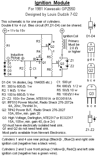
Because the GPZ550 has an inline, 4-cylinder engine, it requires two spark coils, two pickups, and thus, two igniter circuits. This replacement module (as well as the stock unit) actually contains two separate ignition circuits acting independently. In the following analysis, for simplicity, only one circuit will be considered. For a complete module, the circuit need only be doubled. To save on parts, however, it is completely acceptable to have both circuits share the bias section.
Circuit Analysis:
General Description:
The role of the circuit is simply to switch the spark coil's primary current "on" and "off". The control signal is generated by a crankshaft pickup. The pickup gives a signal for Q1 to turn "on". Q1 then turns "on" Q2. Q2 turns "on" Q3. Q3 allows current to flow within the spark coil. When the pickup gives a signal for the spark to occur, Q1 turns "off", then Q2 turns "off", and then Q3 turns "off". When Q3 turns "off", the spark occurs.It is perhaps best to analyze the circuit in reverse, starting at the output.
Selecting Q3, Z1, Z2:
To generate a spark from a spark coil, first a voltage is applied to the primary winding of the coil. This produces a current that increases with time until a maximum current is reached. This current generates a magnetic field. Then the current is switched off abruptly which collapses the magnetic field. The collapsing magnetic field induces a high-voltage (300v to 700v) on the primary winding and a much higher voltage (tens of thousands of volts) on the secondary winding (a.k.a. the high tension winding). The secondary winding produces the spark.In this module, Q3 is switching the current to the primary winding. Q3 is a high-voltage NPN Darlington power transistor. It needs to be able to withstand the high voltage generated in the primary windings of the spark coil. Z1 and Z2 help protect Q3 by clamping the voltage to a safe level for the transistor to withstand.
Q3 is selected as an NTE2317 or ECG2317. It is rated to handle 450v from collector to emitter. This means it can stop primary current in the spark coil when the induced primary voltage is less than 450v. Q3 can handle 15 amps from collector to emitter. It has a power rating of 105 watts. It has a minimum current gain of 40. Due to the design of the Darlington-pair transistor, the forward bias base to emitter voltage is 2 volts.
In order to protect Q3 from induced voltages higher than 450v, Z1 and Z2 are selected as 150v 5w Zener diodes. At first it would appear that Z1 and Z2 are clamping the voltage at 300v. Because Zener diodes have a gradual "knee", they are operating at a higher voltage than their stated rating would indicate. This is because there is a momentary spike of current that gives a momentary high-voltage spike. The sum of the voltage ratings for Z1 and Z2 are 300v, but they are operating at a combined voltage spike of about 450v. Use of higher voltage Zener diodes would result in damage to the NTE2317/ ECG2317.
Selecting R5:
Since Q3 is operating as a switch, it needs to operate in saturation. In saturation, there is the usual voltage drop of about .3v from collector to emitter. With the operating voltage at close to 15v, and coil resistance at 2.0 ohms, the maximum collector current in Q3 (which is also the max. current in the spark coil) is found by:Q3 collector current = (15v - .3v) / 2.0 ohm = 7.35a
Q3 is rated to have a minimum gain of 40. To ensure it is in saturation, a gain of 30 will be assumed. Therefore, the base current in Q3 must be:
Q3 base current = 7.35a / 30 = .245a
To activate this base current, Q2 will be used as a switch (in saturation). Therefore, it will have the typical emitter to collector voltage drop of .3v. As described earlier, Q3 has a base to emitter voltage drop of 2v when conducting current. R6 will temporarily be omitted since its current is almost negligible. Assuming the operating voltage is still 15v, R5 is selected as follows:
R5 = (15v - .3v - 2v) / .245a = 51.8 ohm
For availability purposes, R5 will be selected as 50 ohms. The power in R5 will be significant and is found as follows:
Power in R5 = (15v - .3v - 2v) X (.245a) = 3.1w
To provide a wide safety margin, R5 will be selected as 10w.
Selecting R6:
R6 is the "pull down" resistor for Q3. When Q2 is "off", R6 ensures the base voltage of Q3 is well below 2v to keep Q3 in cutoff. This makes the circuit more stable and helps eliminate unwanted oscillations. 100 ohms works nicely for R6. Because the base of Q3 limits the voltage on R6, there is relatively little current or power in R6.Current in R6 = 2v / 100 ohm = .02a
Power in R6 = 2v X .02a = .04wR6 will be selected as 1/4 w.
With the inclusion of R6 and "rounding off" of R5, some values need adjustment.
Current in R5 = (15v - .3v - 2v) / 50 ohm = .254a
Current in R6 = 2v / 100 ohm = .020a
Q3 base current = .254a - .020a = .234a
Min. Required gain in Q3 = 7.35a / .234a = 31.4This alters the minimum required gain for Q3, but, since it is well below the rated minimum for an NTE2317, it is not a problem.
Selecting Q2:
Q2 is needed to provide gain and a buffer between Q1 and Q3. Q1 cannot directly drive Q3 because the source (s) connection of Q1 must be referenced to ground in order to operate correctly in this circuit. If it directly drove the base circuit of Q3, the reference would be floating somewhere between 0v and 2v.Q2 is a common PNP power transistor. It is available at Radio Shack as a TIP42 power-BJT. The part number is 276-2027. It was chosen because it is cheap and available.
Selecting R4:
When Q2 is "on", its collector current is the same as the current in R5. It was calculated at .254a. In order to get the most reliable switching characteristics in Q1, the current (from drain to source) in Q1 should be minimized. At the same time, the current must be high enough to drive Q2 into saturation. The minimum gain in Q2 is rated at 20. To ensure saturation, the gain will be assumed to be 11 for the purposes of selecting R4.R3 will be temporarily ignored since its current is almost negligible.
The base current for Q2 is found to be:
Q2 base current = .254a / 11 = .023a
When Q1 is "on", the voltage drop from drain (d) to source (s) is found to be .15v. Also, when Q2 is "on", its emitter to base voltage is .7v. The current in R4 is the same as the base current of Q2 (.023a). The value of R4 is found as follows:
Voltage on R4 = 15v - .7v - .15v = 14.85v
Current in R4 = .023a
R4 = 14.85v / .023a = 646 ohm
Power in R4 = 14.85v X .023a = .34wFor the reason of availability, R4 will be selected as 680 ohm. For safety, R4 will be selected as 1/2w.
Selecting R3:
R3 is a "pull up" resistor for Q2. When Q1 is "off", R3 ensures that the emitter-base voltage of Q2 is much less than .7v so that Q2 is in cutoff. This makes the circuit more stable and helps eliminate unwanted oscillations.R3 has a wide range of values which will accomplish the "pull up" function. R3 can be from 100 ohm to 680 ohm. Because of this range, R3 can have another function.
R3 can also be used to determine the point where Q2 starts to turn "on". This is useful for adjusting the dwell angle at idle. However, in order to do this, the actual value of R3 must be determined by building the circuit and experimenting with values while the circuit is in operation. This is the only way to compensate for different tolerances among transistors and resistors. This requires running an actual engine or devising a test machine, much like the old days of using a distributor test machine. Hooking up an oscilloscope or a dwell meter to the negative of the coil will show the dwell angle. At idle, about 80 to 90 degrees (crankshaft) is desired. The dwell should increase to a maximum of 120 degrees (crankshaft) by 2500 RPM and up. Also, for start up, the dwell should be around 20 degrees (10 msec) at 300 RPM. It should be noted that the air gap between the pickup and the rotor will also affect the dwell, so this is part of the setup as well. Since the ignition module for the GPZ550 consists of two circuits. R3 may be different for each circuit in order to produce the same performance in each circuit. A smaller R3 resistor value will decrease the dwell angle and vice versa.
For general usage, it is satisfactory to simply use a midrange value of 390 ohms as R3. R3 uses very little power so it is a 1/4 w resistor.
For this analysis, R3 will be selected as 390 ohms. With the inclusion of R3 and the "rounding off" of R4, some values need adjustment:
Current in R4 = 14.85v / 680 ohm = .022a
Current in R3 = .7v / 390 ohm = .002a
Q2 base current = .022a - .002a = .020a
Min. gain in Q2 = .254a / .020a = 12.7This alters the minimum required gain for Q2, but, since it is well below the rated minimum for a TIP42, it is not a problem.
The rest of the circuit consists of the signal input section and requires some background information.
Pickup Signal:
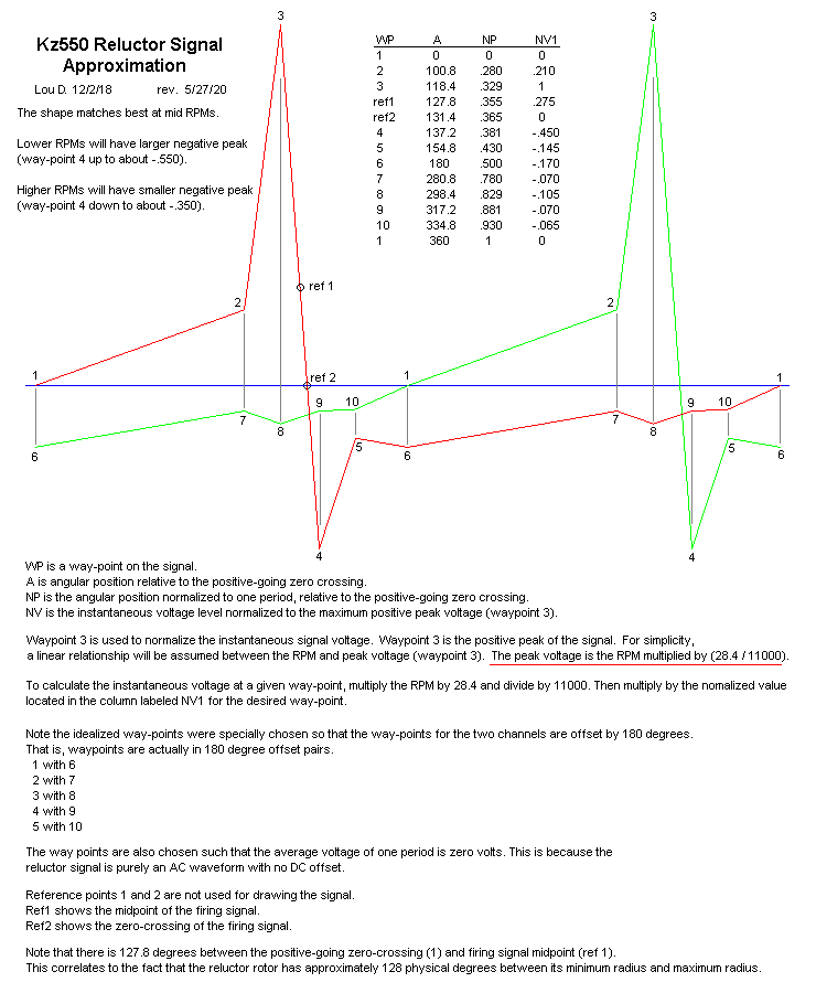
An inductive pickup coil generates the ignition control signal. It has a DC resistance of 450 ohms and an inductance of 350 mH.The inductive pickup is mounted next to the rotor which is mounted to a mechanical advance mechanism. The mechanical advance mechanism is mounted to the end of the crankshaft.
The pickup is simply a coil of wire with a pole piece going through the center of it. A permanent magnet provides a magnetic field that passes through the center of the pickup coil and to the iron rotor. As the rotor spins, it comes closer to and farther away from the pickup. This generates a positive and negative voltage respectively.
During one rotation of the crankshaft, the rotor produces a single positive wave for 120 degrees followed by a single negative wave for 240 degrees.
The positive wave starts with a gradual increase in voltage. As the point of the rotor approaches the pickup, a sharp positive spike is generated. When the point of the rotor passes the pickup, the sharp positive spike changes to a sharp negative spike. The negative signal then gradually increases to approach 0 volts. Then the positive wave begins again.
The amplitude of the signal increases greatly with RPM.
Selecting R1, D1 - D4:
The bias section simply creates a steady voltage to be supplied to the pickups so their signals will sufficiently drive the input MOSFET. R1 and D1 to D4 make up the bias circuit. R1 is given a range due to the nature of tolerances in diodes and MOSFET thresholds.The power supply is 15 volts.
Q1 energizes the rest of the circuit and the spark coil when the voltage applied at the gate (g) of Q1 exceeds the threshold voltage.
Since the gate threshold of Q1 is just above 2.9 volts, the pickups must be biased to 2.9 volts. This simply means the negative side of the pickup receives a steady 2.9 volts DC.
The bias voltage is created by using a series of forward biased diodes with a current limit resistor. Since there is virtually no current flow in the pickups, the pickups don't affect the bias voltage.
D1 to D4 are small 1A diodes. If each diode D1 to D4 has a forward voltage drop of .72 volts at .0356 amp, then the four diodes together will have a voltage drop of 2.88 volts at .0356 amp.
4 X .72v = 2.88v
R1 is the current limiter for the diodes. R1 is found as follows:
Voltage on R1 = 15v - 2.88v = 12.12v
Current in R1 = .0356a
R1 = 12.12v / .0356a = 340 ohm
Power in R1 = 12.12v X .0356a = .4wR1 should be 340 ohms. For a safety margin, R1 will be a 1w resistor. Two 1/2 w, 680 ohm resistors in parallel work well as a substitute.
If the bias voltage is too high, the circuit and spark coil will be energized even when the pickups are not producing any signal (i.e. the engine is stopped). This will overheat the circuit and spark coil, and thus, should be avoided by reducing the bias voltage.
It should be noted that the bias circuit can be shared by several ignition circuits thus reducing the part count. For a multi-cylinder engine with multiple spark coils, the negative terminals of the other pickup would attach at the same point (between R1and D1).
Selecting Q1:
The input device is the power MOSFET Q1. It is an IRF510 which is readily available at Radio Shack. The part number is 276-2072a. It was chosen for it's very high input impedance and durability. It is not being used to handle any significant current, voltage, or power so it should be very reliable.The high impedance input minimizes the current in the pickups. This is required because the pickups are inductors and any current will be significantly delayed. This, in turn, would delay the spark.
When the input signal from the pickup is positive enough to overcome the threshold voltage, the circuit and spark coil become energized. This begins the dwell period. When the point of the rotor passes the pickup and the signal changes from positive to negative, the circuit shuts down and the spark coil produces a spark. This ends the dwell period.
The dwell period is affected by the amplitude of the positive signal. The signal voltage is determined by the rotational speed of the rotor. At low RPM, only the spike has enough voltage to create the dwell period, thus, the dwell angle is small. At high RPM, the entire positive signal is strong enough to create the dwell period, thus, the dwell is the full 120 degrees. This is a simple way to have a variable dwell angle.
Selecting R2:
Runaway oscillations can occur when the connection to the pickup is lost. This leads to the destruction of Q3. By grounding the gate of Q1 through R2, these oscillations can be prevented. R2 is selected as 1 MegaOhm, 1/4 w. 1 Meg is used so the current in the pickup will remain minimal. There is no power involved to speak of.Selecting C1:
C1 attenuates some of the noise at the input stage.C1 also performs another task. The pickup signal goes from positive to negative when the spark is to be fired. At low RPMs, the change happens slowly enough that a brief oscillation can occur during the transition from pos. to neg. This oscillation bleeds energy from the spark coil. C1 helps to reduce the oscillation.
C1 was selected to be 500pf through experimentation. If C1 is much larger than 600pf, it will start to increase the current in the pickup and a noticeable delay will develop. 900pf should be the absolute maximum for C1. At 900pf, a delay of 1 or 2 degrees will be seen at around 7000 RPM and gets worse at higher RPMs.
Performance note:
During experimentation, one odd behavior was noticed. At very high RPMs (above 7500), there is a slight firing delay. This delay increases and approaches 4 degrees (crankshaft) by 10,000 RPM. This also occurs with the stock ignition module. It seems to be a characteristic of the inductive coil in combination with an input impedance of the module being less than the ideal value of infinity. It seems to be the one drawback of using an inductive pickup instead of optical or Hall-effect pickups.Packaging:
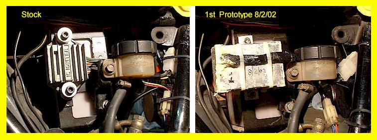
The entire circuit was hand assembled onto a general purpose circuit board and soldered point to point. Then the entire circuit was placed into an aluminum project box. The NTE2317 transistors (Q3) were mounted to the inside walls of the aluminum box with a supplied Mylar electric insulator and thermal transfer paste to provide a heat sink. In operation, the heat given off by Q3 was relatively mild. It never became too hot to touch.Other Designs:
During the development of this project, the circuit underwent various changes. Some previous designs were ruled out for having some serious drawbacks. Here are some of the notable ones.Op-amp input:
The first design attempted used a 741 op-amp as the input device. The circuit worked rather well. The op-amp had the very high input impedance required. The only problem with the op-amp was the fact that it was very susceptible to radio interference and mechanical noise. A nearby radio transmitter would cause the op-amp to go into severe oscillations and the spark would cease completely. Any mechanical noise would be picked up and amplified by the high gain of the op-amp which would cause false triggers and false sparks to occur.BJT input:
A BJT was later tried as the input stage. This design also initially appeared to work. The problem with a BJT is that it required significant current in the pickup in order to operate. Due to the nature of inductors (which is what the pickup is), the current lags behind the voltage in the pickup. As RPMs increased, the lag increased (in terms of crankshaft rotation). The spark was delayed enough such that the engine would not rev above 5000 RPM regardless of load. With no load, this engine should easily rev to 11,000 RPM. A timing light showed that the spark was delayed approximately 20 degrees from where it should have been firing.Capacitor feed back:
In order to create a hysterisis effect for eliminating unwanted oscillations during the firing signal, several capacitor-coupled feedback loops were experimented with. However, none of them proved useful for various reasons.Anything coupled to the input would alter the input impedance and would, thus, cause a delay in the timing.
The output had many natural oscillations due to the "ringing" in the spark coil. This would cause wild oscillations in the feedback loop.
In the end, the best result was from using no feedback loop at all.
Conclusion:
This ignition module was installed on a GPZ550 motorcycle and a KZ650 motorcycle. Performance seemed to improve slightly over the stock ignition module. This was unexpected. This may simply be due to smoothness over the stock unit. With a timing-light, it was evident that the stock unit had the occasional false trigger. The project module did not seem to have this problem.Reliability testing is still in progress with no failures of any kind. The module currently has several thousand miles on it as of 12/2004.